Samsung reportedly turns to TSMC's 3nm process for NVIDIA's NVHBM
Samsung has reportedly agreed to use TSMC to manufacture the base die for NVIDIA's custom NVHBM memory, departing from its usual practice of handling both core and base dies itself. NVIDIA wants Samsung, Micron and SK hynix to use the same manufacturing process to deliver consistent performance and reduce qualification work.
 Layla Haddad
A shared process for custom memory
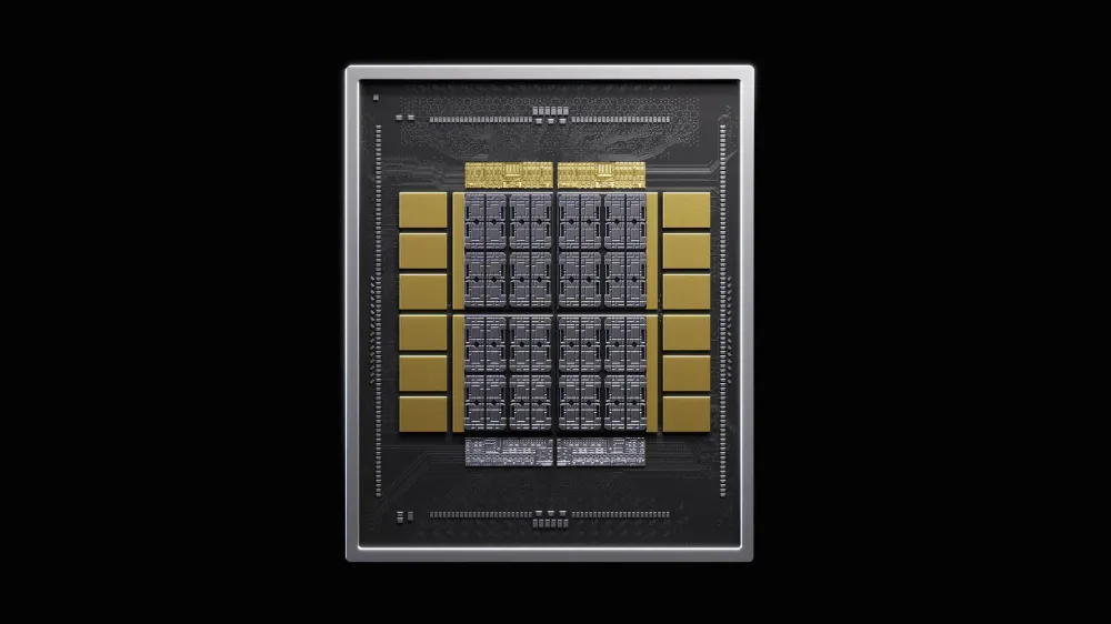
According to Wccftech's report, NVIDIA has requested TSMC's 3nm process for NVHBM base dies across all three memory suppliers. The core dies are to use sixth-generation DRAM technology, known as 1c. Standardizing production would spare NVIDIA from separately verifying each supplier's samples.
Samsung has reportedly accepted the arrangement, marking its first departure from its turnkey approach to HBM production. The change brings Samsung and foundry rival TSMC together on the base die for NVIDIA's custom memory.
A separate claim about TSMC's role has drawn a denial. An update to the report said NVIDIA had also asked TSMC to begin producing 3D DRAM, beyond manufacturing the NVHBM base die. TSMC denied having plans to mass-produce 3D DRAM and said it would remain focused on logic chips.
NVIDIA's performance claims and early adoption
NVHBM has been linked to NVIDIA's Feynman GPUs. NVIDIA says the memory can provide up to 30% more bandwidth than standard HBM4E while drawing up to 15% less power.
The design moves the memory controller into the 3D HBM stack and incorporates a custom PHY. According to NVIDIA's Technical Blog, this cuts PHY and support area by up to 67% relative to the JEDEC HBM4E standard. NVIDIA cites up to 25% more compute die area on the XPU and up to 30% more main-die silicon. It claims the combined bandwidth, area and power improvements can raise overall end-to-end performance per XPU by up to 30%.
Despite NVIDIA's effort to standardize production among suppliers, NVHBM is a company-specific technology, not a JEDEC industry standard. Blocks & Files reports that JEDEC has made no public comment on it and notes that NVIDIA's Barry Wagner chaired the HBM subcommittee when JEDEC announced HBM4.
NVIDIA offers NVHBM through its NVLink Fusion program. Amazon's Annapurna Labs supports the technology as an NVLink partner, making it an early adopter.
Samsung keeps its own manufacturing options
The TSMC arrangement does not extend to all of Samsung's HBM business. Seoul Economic Daily reports that Samsung will continue making both core and base dies for standard HBM4 and HBM4E, with the base dies using its own 4nm foundry process. It will also retain the turnkey model for custom HBM sold to other customers, including AMD.
For NVHBM, Samsung is validating its own 2nm process as a possible alternative if demand exceeds TSMC's capacity. Industry yield estimates reported by Seoul Economic Daily and carried by The Next Web in October 2026 put TSMC's 3nm yield above 90%, compared with roughly 60% for Samsung Foundry's comparable 2nm SF2 process.
HBM is also helping reduce Samsung's foundry losses, according to an earlier estimate cited by Wccftech. That estimate put the 2026 loss at 3.92 trillion won, or about $2.95 billion, down 41% from 6.74 trillion won, or about $5.1 billion, in 2025.
Demand forecasts and TSMC's expansion
NVIDIA's purchasing scale helps explain its influence over the manufacturing arrangement. Blocks & Files, citing reported Morgan Stanley data, says NVIDIA is expected to buy 37% of the world's HBM supply in 2027, giving the three suppliers a reason to accept its choice of foundry process for NVHBM base dies.
The broader HBM market is expected to remain tight. According to Seoul Economic Daily, UBS forecasts 2027 demand of about 61.5 billion gigabits, a 91% year-over-year increase. Projected new shipments from memory manufacturers total only 54.6 billion gigabits, leaving an estimated shortfall of roughly 10%.
TSMC is adding two 3nm production lines at Fab 18 in Tainan, according to Seoul Economic Daily as reported by The Next Web. Mass production is scheduled to begin on one line in the first half of 2027 and on the other in the first half of 2028. TSMC also plans 3nm lines at its second plants in Arizona and Kumamoto, Japan.